

Graphene Nanoplatelets


Graphene Nanoplatelets
Main Features
- CAS Number – 7782425
- Appearance – Blackish colour powder
- COA – C – >99% & O < 0.5%
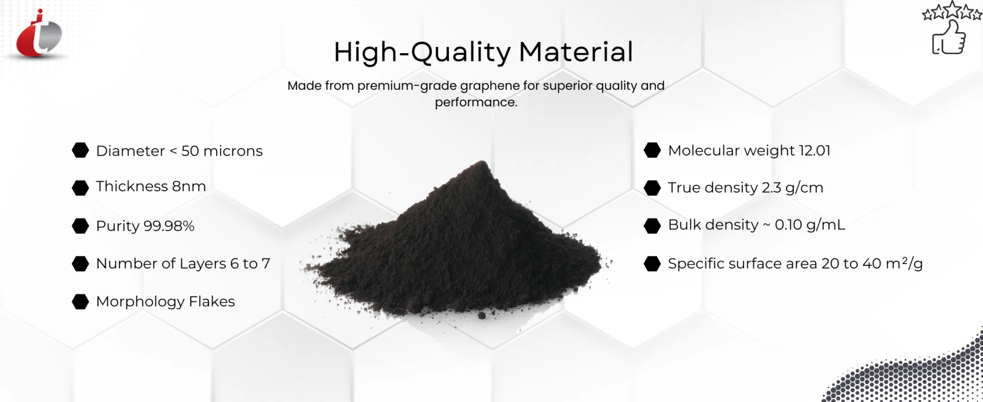
- Diameter – < 50 microns
- Thickness – 8nm
- Purity – 99.98%
- Number of Layers – 6 to 7
- Morphology – Flakes
- Molecular weight – 12.01
- True density – 2.3 g/cm3
- Bulk density – ~ 0.10 g/mL
- Specific surface area – 20 to 40 m2/g
Full Description of Graphene Nanoplatelets
Graphene nanoplatelets(GNPs) manufactured from graphene, an innovative and revolutionary material discovered in 2004. The nanoplatelets form with the multiple layers, where the thickness in nanometers and diameter in the microns. These layers are attached each other by strong Van Der Waals force of attraction.
Graphene made when carbon atoms came together to form bonds with each other and made a hexagonal-shaped, latticed, honeycomb-like structure. In this, each carbon atom shares its individual electrons, apart from one electron, with three different carbon atoms. This forms a stronger bond between the carbon atoms, while the single free electron (also called the Pi electron) is able to conduct electricity efficiently over the graphene surface.
Graphene Nanoplatelets Process
Various methods are needed to form this lattice-shaped carbon structure into sheets, tubes, and many more products. Graphene nanoplatelets are one such derivative of conventional graphene and are around 5-10 nanometers in size with the maximum thickness of 50 microns only. This used in a research as well as industrial sectors. It is comes in a form of flakes powder and dispersed form as per need. The functional group nanoplatelets like carboxylic (COOH), Amine (NH2), F and N2 can be produced as per clients requirement. It added in the polymers like rubber, nylon, and plastic to improve conductivity, tensile strength, corrosion resistance, stiffness, mechanical reinforcement, hardness and gas barrier properties. The incorporation percentage in polymer varies from 2 to 10% as per applications.
Graphene nanoplatelets included in the range of advanced materials known to science. It is also known by graphene nanoparticles. These are microscopically tiny stacks of graphene which is set to replace conventional electronic components made from silicon. Graphene is also known as the ‘wonder material’ due to its immensely impressive properties, such as highest tensile strength, and excellent electrical and thermal conductivity.
| Technical Specifications of Graphene Nanoplatelets (GNPs) | |
|---|---|
| Product Name | Graphene Nanoplatelets (GNPs) |
| Material | Graphene Nanoplatelets / Graphene Nanoparticles |
| Chemical Composition | Carbon (C) |
| CAS Number | 7782-42-5 |
| Appearance | Blackish Powder |
| Morphology | Flakes / Platelets |
| Purity | 99.98% |
| Carbon Content | >99% |
| Oxygen Content | <0.5% |
| Number of Layers | 6–7 Layers |
| Thickness | Approximately 8 nm |
| Platelet Diameter | <50 µm |
| Specific Surface Area | 20–40 m²/g |
| True Density | 2.3 g/cm³ |
| Bulk Density | Approximately 0.10 g/mL |
| Atomic / Molecular Weight | 12.01 g/mol |
| Electrical Conductivity | Excellent |
| Thermal Conductivity | Excellent |
| Mechanical Reinforcement | Excellent |
| Aspect Ratio | High |
| Functionalization Options | Carboxyl (-COOH), Amine (-NH₂), Fluorinated and Nitrogen-Functionalized Grades Available |
| Polymer Incorporation | Typically 2–10%, Depending on Application |
| Compatible Matrices | Rubber, Nylon, Plastics, Polymers, Metals and Composite Materials |
| Available Forms | Powder / Flake and Dispersed Form |
| Typical Applications | Conductive Composites, Batteries, Supercapacitors, EMI Shielding, Conductive Inks, Thermal Management, Coatings, Automotive, Aerospace, Fuel Cells and Polymer Reinforcement |
Download Resources

Applications of Graphene Nanoplatelets
Graphene nanoplatelets are finding increasing application in numerous industries, including:
- Transport industry – Use as metal-matrix, lightweight composites/alloys for lighter vehicle body parts, efficient lubricant, embedded antennas/electronic circuits, manufacturing super-capacitors, lightweight Li-Ion batteries.
- Energy industry – Use as power buffer between the wind turbine and electrical grid, large-scale, advanced batteries and prolonged power storage, bi-polar plates/catalysis materials for fuel cells, replacement of conventional, bulky and heavy Li-Ion batteries with alternate lightweight and more powerful battery components.
- Electronics industry – Use in the manufacturing of conductive ink for printing electronic circuits on fabric/material/surface, thermal coating for efficient dissipation of heat, coating for anti-EMI capability and conductive circuits for LED back-panels.
- Aerospace industry – Use in the manufacturing of lightweight composite materials for aircraft body parts, anti-lightening protection through conductive sheets, and enhanced impact resistance.
- Infrastructure industry – Use in development of optimally strong concrete for making taller buildings and bridges, abrasion-resistant cement for warehouses and roadways, inexpensive embedded stress sensor technology, efficient membranes for water purification, cleansing agent for resolving oil-spill effects.
- Apart from these, graphene nanoplatelets are also finding potential use in defence systems, biomedical and the sports industry too.
| Parameter | Graphene Nanoplatelets (GNPs) | Graphene Powder | Graphene Oxide (GO) | Reduced Graphene Oxide (rGO) | Multi-Walled Carbon Nanotubes (MWCNTs) |
|---|---|---|---|---|---|
| Material Structure | Stacked Graphene Platelets | Few-Layer Graphene Sheets | Oxidized Graphene Sheets | Reduced / Partially Deoxygenated Graphene Sheets | Concentric Graphitic Nanotubes |
| Morphology | Flakes / Platelets | Exfoliated Sheets / Powder | Thin Oxidized Sheets | Wrinkled / Reduced Graphene Sheets | Tubular Nanostructure |
| Purity | 99.98% | >99% | >99% | >99% | 99–99.99% |
| Number of Layers / Walls | 6–7 Layers | 4–6 Layers | 2–6 Layers | 3–6 Layers | 4–8 Walls |
| Thickness / Diameter | ~8 nm Thickness | ~3–4 nm Thickness | 3–5 nm Thickness | 0.8–2 nm Thickness | 10–15 nm Outer Diameter |
| Lateral Size / Length | <50 µm Diameter | 5–10 µm | 5–10 µm | ~10 µm | ~10 µm Length |
| Specific Surface Area | 20–40 m²/g | ~150 m²/g | >110 m²/g | >150 m²/g | 330–400 m²/g |
| Bulk Density | ~0.10 g/mL | 0.24 g/cm³ | 0.48 g/cm³ | 0.121 g/cm³ | 0.20–0.35 g/cm³ |
| Electrical Conductivity | Excellent | Excellent | Low | High | Excellent |
| Thermal Conductivity | Excellent | Excellent | Moderate | High | Excellent |
| Water Dispersibility | Limited | Limited | Excellent | Moderate | Limited Without Functionalization |
| Polymer Reinforcement | Excellent | Excellent | Very Good | Excellent | Excellent |
| EMI Shielding | Excellent | Excellent | Moderate | Excellent | Excellent |
| Energy Storage Applications | Excellent | Excellent | Good | Excellent | Excellent |
| Conductive Coatings | Excellent | Excellent | Limited Without Reduction | Excellent | Excellent |
| Composite Processing | Excellent for Bulk Composite Applications | Very Good | Excellent Due to Dispersibility | Very Good | Good but Requires Effective Dispersion |
| Typical Applications | Composites, EMI Shielding, Batteries, Conductive Coatings, Automotive & Aerospace | Sensors, Batteries, Conductive Inks, Electronics, Composites | Biosensors, Membranes, Coatings, Water Treatment, Functional Materials | Energy Storage, Conductive Coatings, Sensors, Anticorrosion Materials | Batteries, EMI Shielding, Conductive Polymers, Sensors, Aerospace Composites |
| Best For | Large-Area Conductive & Reinforcing Additives | High-Performance Graphene Research | Functionalization & Water-Based Processing | Conductive Functional Graphene Applications | High-Aspect-Ratio Conductive Reinforcement |
| Key Advantage | Excellent Balance of Conductivity, Reinforcement & Processability | High Surface Area & Graphene Performance | Excellent Dispersibility & Surface Functionalization | Improved Conductivity with Functional Surface | Extremely High Aspect Ratio & Mechanical Reinforcement |
Why Choose Graphene Nanoplatelets?
- High purity of 99.98% for research and industrial applications
- Excellent electrical and thermal conductivity
- Flake morphology suitable for conductive network formation
- Excellent reinforcement for polymers and composite materials
- Suitable for EMI shielding and antistatic applications
- Useful in batteries, supercapacitors and energy storage systems
- Can improve mechanical strength, stiffness and barrier properties
- Functionalized grades can be produced for specialized applications
Characterization Data


Why Techinstro?
Techinstro has been the prominent graphene-nanoplatelets (GNPs) supplier to leading industrial players all over the world. The price varies as per the quantity of product purchased. If the volume increases, the cost of the product decreases. The brand is renowned for being the top graphene-nanoplatelets manufacturers and distributors worldwide including India, China, Africa, US, UK, South America and Australia.
FAQ's
They are manufactured from graphene and formed into multi-layer nanoplatelets held together by strong Van der Waals forces.
Screen printing is not done directly with the nanoplatelet powder; it is achieved using our graphene ink instead.
Nanoplatelets are multi-layer flake stacks (6–7 layers) with the thickness measured in nanometres and the diameter in microns.
Yes, the free Pi electron gives it excellent electrical conductivity, and it is tuneable from an insulator to a conductor.
It is supplied as a flake powder or in a dispersed form, and while it is not readily water-soluble on its own, a suitable dispersion medium can be provided on request.
Its purity is 99.98%, with a COA of C greater than 99% and O less than 0.5%.
The diameter is less than 50 microns, and the thickness is 8 nm.
It has 6 to 7 layers.
Its specific surface area is 20 to 40 m²/g.
Its true density is 2.3 g/cm³, and its bulk density is around 0.10 g/ml.
It is a blackish-colour flake powder.
Yes, functionalized grades with COOH, NH₂, F, and N₂ groups are available on request.
It is mainly used in composites, batteries and supercapacitors, conductive inks, aerospace, and infrastructure.